A few weeks ago I put out an article that touched a few of the main differences between cheaper lenses and higher-end lenses.
What wasn’t really included in that list was why mechanically and optically higher-end lenses out of Japan are so superior to what these newer companies are able to produce.
While I’m not a lens designer or even an engineer, I do like to read about this stuff and I am regularly schooled by readers of this blog in the comment sections, so I have learned a lot over the years.
Recently I found something cool I thought I would share regarding what’s going on with those Sony GM lenses.
Sony recently released a new GM 50mm f1.2. This was a lens that for a long time people say Sony could not make because their full-frame camera essentially uses an APS-C mount, which I never fully bought. The reason is, it’s all about the angles and distance from the point of convergence of the light to the sensor and even with the Sony E mounts smaller mount, this geometry is still superior to any DLSR. In other words, even though Sony uses a small mount, they should still be able to optically outperform, or at least do more things than any of the DSLR competitors.
This is not a Sony fan-boy article, it is just easiest to find information around Sony products because they are the only camera company that doesn’t suck at marketing. So they release stories by their designers that make their products seem awesome and high-tech for us nerds. Maybe Nikon or Canon has similar processes, but we’ll never know – because they don’t do a good job at catering to us techies.
How Did Sony Get The 50mm f1.2 So Small? XA Elements
There are a few tricks lens designers are using now to make lenses smaller. Often they use advanced plastics or resins, to keep elements smaller and lighter. Often these are just used in Aspherical elements because they can have such a high index of refractions. I believe this allows them to make smaller and lighter elements vs glass but that perform the same function.
Now, what I wanted to know, was how Sony was able to keep the 50mm f1.2 so small while maintaining decent performance.
Don’t get me wrong, it’s still a thick boy, but it’s just significantly smaller and lighter than Nikon’s 50mm f1.2, so it had to be from some new optics with some new aspherical elements, or some design decisions to allow for compromises in IQ for the smaller size. Knowing Nikon and Sony, it’s probably the latter.
Anyway, I found some cool stories by Sony lens engineers.
You can read them all here at Sony’s website.
I will summarize the points I like.
Sony Lens Designer Stories – These Are Cool
The Sony 50mm f1.2 GM uses three XA elements, Sony doesn’t really touch on the specs of these elements just that they are hybrid designs of resin surfaces formed around the spherical glass.
By the way, those that don’t know the history of Sony cameras and lenses, they came out of the acquisition of the Konica Minolta, camera and lens division. For those that say Sony is not a camera company, well, Minolta has been around since 1928 as a Japanese / German company.
Sony has been designing their own lenses even before that acquisition with which is validated by this quote from Hitoshi Nakanishi, a Sony lens engineer when talking about aspherical lenses.
Hitoshi Nakanishi: “The history of Sony’s aspherical lens development dates back some 20 years”
and.
“. . . we first had to build some technology for processing small lenses with high precision, and then we gradually stepped up to larger lenses as we established a mass production system.”
And Toshihiro Masuda mentions that the whole aspherical lens development and mass production system had to be built out from scratch. They had to build the machines to evaluate the machines that make the glass.
Now after 20 years they have some pretty crazy technology and these new XA elements are hybrid in design which Masuda talks about there.
Masuda: We called it a hybrid lens since it employed resin aspherical surfaces on spherical glass. To tell you the truth, though, that first run was a failure.
…
“We ended up taking about a year to identify all the concerns and then improve the manufacturing equipment and processes to resolve the overall problem.”
It took them 10 years to transition to molded glass aspherical elements.
“it would have been cheaper to buy the lenses from another company. However, management decided that we should expand Sony’s own optical technologies even if it would cost some money. So we continued to do R&D into molded glass lenses while mass producing the hybrid lenses.”
They also had to develop an improved process to grind down and polish these aspherical elements so that they wouldn’t exhibit characteristics of onion ring bokeh, which you can see on a lot of older Fujifilm lenses.
Masuda: “. . . it is also necessary to perform grinding and polishing on the nanometer order . . . We have put a lot of creativity into addressing this issue by combining elements such as tool diameter and rotation pitch in order to reduce grooves as much as possible or to make them in a way that is easy to polish out. In this way, we were able to grind at a high level of precision to eliminate deviations in the lens shape.”
Who the whole process of establishing the manufacturing technology of these new XA elements took Sony 20 years.
There are a few more cool pieces of information I pulled from these interviews.
This is from Nakanishi who is in charge of the XA lens designs.
Nakanishi: “… I work on developing the optical glass material, developing new lens shapes, developing the die, and designing the casting process. Most people would not imagine, but there are more than 200 kinds of optical glass materials in the world. Only some of them, however, can be processed into aspherical lenses”
Why Copy-to-Copy Variations Is Better With High-End Lenses
Precision lenses have to have a very small tolerance of error and have some temperatures that are off by just a half of a degree in the manufacturing process can throw everything off.
The designs have to be stable with mass production where there is very little change between each element out of the thousands that are produced and this process is extremely difficult.
Actually, this is one of the great feats Nikon has accomplished with their new manufacturing process of the Z mount lenses.
Here a Sony Engineer who is in charge of the manufacturing technology talks about this.
Masuda . . . In developing a lens fabrication process, there is a base process, and then I customize it for each purpose. That is, even if the same glass material is molded under the same conditions, it won’t necessarily come out as intended if the lens shape is different . . . So, the recipe for the fabrication process is different for each lens, and a great deal of trial and error is needed to finally achieve stable mass production.”
He also talks about working with the designer to change the specs of the lens so that it’s better suited for mass production. So they will literally change the design for mass production, and this is actually pretty standard across every industry.
Nakanishi: “Since the glass elements differ from lens to lens, stamping conditions such as molding temperature, pressure, and cooling time are different for each type of lens. There are so many forming parameters to be considered, and there are innumerable combinations, so it takes a very long time to figure out the optimal process conditions.”
Masuda:”Glass material repeatedly expands and contracts, so it is pretty difficult to perfectly transfer the shape of the die. For example, even at temperatures of 600°C or higher, a mere 0.1°C difference can lead to an error in the precision of the lens.”
And actually, Sony had to design its own temperature measuring devices to fine-tune this process.
Brands Outsource Lens Design Sometimes
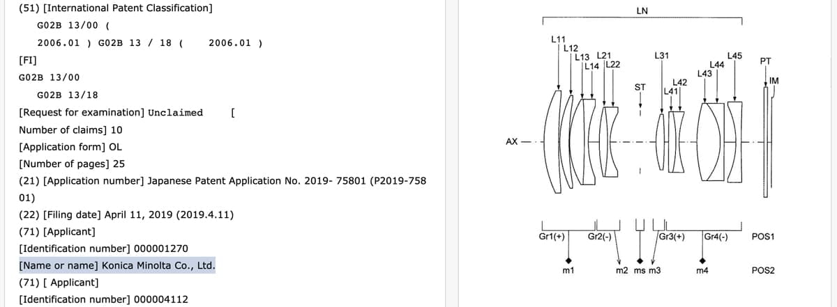
What else is interesting is Minolta is still around today, and that they actually do assist in lens designs according to a Nikon lens patent.
I’ve always wondered how much technology all these companies share and how much do they outsource development resources.
Turns out they do it a lot.
One of the Sony engineers talked about elements from a third-party but Sony was willing to invest in doing more internally.
You’ve probably seen me allude to this a few times based on assumptions. It’s just too much of a coincidence that Canon and Sony start releasing lenses with never used before / brand new control rings only weeks apart from each other.
There were even rumors for a while that Canon had a hand in some of Sony’s design that I’ve personally heard, which might just boil down to only meaning they are sharing patents, who knows, it doesn’t matter.
What is cool is here, in this Nikon Z 85mm patent, it is written that the lens was developed together with Konica Minolta.
So it would seem a division of Konica Minolta that does lens design is still around and available for hire. Meaning there is a high probability that Sony, Canon and Nikon probably all go to them to outsource some lens design. Which would make sense, they’ve all released an insane number of lenses these last few years.
Or it’s possible, they invest money in third-party companies to see if they can come up with a better design to put some pressure on the internal team. This happens a lot in the movie and game trailer world where a studio will hire out a few trailer houses to do the same trailer where they then take the best parts from all the different edits and combine them into one.
Historically, Fujifilm has been designing Hasselblad lenses, and Tokina would design the Pentax lenses and even right now, some of those Tokina and Viltrox lenses use the same optical formulas.
So before we all run out and say, Sony makes the best lenses or Nikon makes the best lenses and so on, there is a high probability that you might be comparing two lenses that are actually designed by the same team, are sharing patents or using elements from another brand.
Cameras Are All The Same Too
Just like with our cameras. Components come from all over the place. Nikon might design a sensor, the Silicon might come from Tower Jazz with the manufacturing or assembly done with Sony, which uses machines, built by Nikon.
When you buy a camera or lens, you are buying a product made by a shared ecosystem.
Inside the cameras, there is a brain called a processor, our cameras today use ARM processors (owned by Softbank, with an attempt acquisition by Nvidia).
Canon historically has used Texas Instruments Arm Processors. Nikon today has been using the Socioinext Milbeaut ARM processors, manufactured at TSMC or by Samsung – heavily customized of course. And I’m not sure who Sony and Fujifilm use.
Some of these sensor fab companies are even using machines built by Nikon, Canon or ASML. Although ASML has the monopoly right now for EUV lithography. It’s who TSMC uses, and who Intel is transitioning to from Nikon.
My point is, these narrative people are always pushing that one camera company is superior to another based on technology is dumb. It’s not about the tech, but about the art of the camera design, the economics, and marketing.
Nikon and Fujifilm have access to everything Sony and Canon have and vise versa. The only limitation is what the Fab companies can produce, TSMC or Samsung and the current ARM architectures that are available at the time. Not only that, they all provide each other with machines that build the machines.
The rest comes down to economics, how much money are they will to spend on a more advanced processor with more advanced cooling systems compared to the competition.
For example, you cannot put H.265 into your camera unless you add the hardware for the encoding or decoding. This might come built into the processor or you might have to add it separately. Plus, there are something like 500 patents based around H.265 which means you have to license and pay for that patent pool and it may not be cost-effective to put it into every system.
Another example is PCIe 2.0 cameras will not see a significant gain by switching from XQD to CFexpress memory cards, since your bottleneck is still single-lane PCIe 2.0. Unless you add another processor / another lane. You won’t be able to upgrade to PCIe 3.0, unless the ARM processors are offering that at a reasonable price.
What is still very strange to me is that the screen on the $850 Fujifilm X-E4 consumer camera is superior to the screen on the $6,500 Sony A1. I have not been able to figure out why Sony still sources cheap screens for their high-end cameras, it makes no sense.
Now hopefully Google doesn’t rip me a new one for using that many quotes from another website.









Leave a Reply